


Advertisements
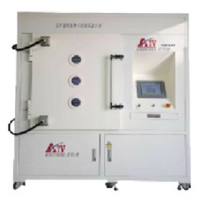


Horizontal Plasma System AH-V1000
| Price: | US$ 57000 / Set |
|---|---|
| Minimum Order: | 1set |
| Payment Terms: | 30%T/T in advance, 70% T/T before shipment |
| Port of Export: | SHANGHAI |
Product Details
| Model No.: | AH-V1000 | Brand Name: | ATV |
|---|
| Certification: | |
|---|---|
| Specification: |
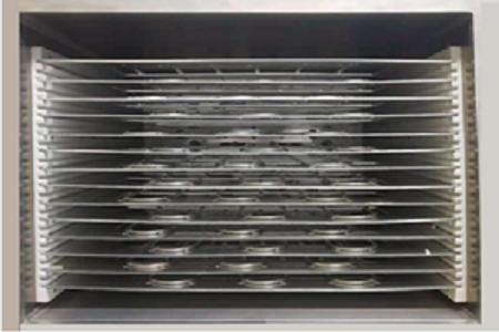
1.Outline Dimensions (footprint):1850*1800*2100H mm 2.Vacuum chamber size:1450*670*950mm 3.Maximum Treatment Area:1290*570mm 4.Maximum number of processing layers:13 layer 5.Input voltage:3-Phase 380 VAC~440V, 50 Hz/60 Hz 6.Output frequency:40KHz 7.Output power:10Kw 8.Discharge vacuum:20Pa-80Pa 9.Loadable Gases: O2, N2, H2, CF4 10.Treatment Time for Each Batch: 15~30 minutes |
Packaging & Delivery
| Packaging: | simple water-prof packaging or customise with vacu |
|---|---|
| Delivery/Lead Time: | 60 days |
| Production Capacity: | 30 set per month |
Product Description
Search Keyword: PCB Plasma Desmear
FPC Plasma Desmear
IC substracts Plasma treatment
LCD Plasma Cleaning
PTFE Plasma treatment
Plasma treatment is an effective surface processing solution for various materials, including resins, ceramics, metals, and composite materials. It is widely used for contaminant removal, desmear and etch-back, carbon removal, and PTFE surface activation. These treatments enhance material properties and increase surface energy, resulting in better adhesion and durability. This is crucial for a wide range of industries, such as PCB and HDI manufacturing, semiconductor packaging, medical device processing, and automotive decoration cleaning.
The AH-V1000 plasma system is designed based on years of close collaboration with PCB manufacturing plants and users from other industries. With its outstanding treatment uniformity and environmentally friendly process, the AH-V1000 is a mature solution that meets the process requirements of these diverse application fields.
Features & Performance:
1.Suitable for large quantities of PCB/FPC and other products across a wide range of applications.
2.Short processing time and high efficiency to improve production capacity.
3.Extremely simple and convenient operation, with low usage costs and easy maintenance.
4.Dry process with no residue left on the product surface after treatment, ensuring no discharge of pollutants and providing a safe and environmentally friendly solution.
Merits:
Environmentally friendly molecular-level surface cleaning enhances uniformity and hydrophilicity, making it an ideal pre-treatment for bonding processes.
Application fields:
Suitable for PCBs,FPC, IC substrates, LCDs, PV batteries, semiconductors, PTFE, automotive interior parts, medical equipment, plastic and rubber products.
|
SUPPLIER PROFILE
|
|||
|---|---|---|---|
| Company: | Suzhou ATV Electronic Technology Co., Ltd | ||
| City/State | kunshan, Jiangsu | Country: |
China 
|
| Business Type: | Export - Manufacturer / Trading Company | Established: | 2011 |
| Member Since: | 2024 | Contact Person | Lance Xu |
SUPPLIER PROFILE
City/State/Country -
kunshan, Jiangsu
China
Business Type -
Export - Manufacturer / Trading Company
Established -
2011
Member Since -
2024
Contact Person -
Lance Xu